Sapphire substrates(Al2O3 substrates)
Sapphire (Al2O3) has good thermal properties, excellent electrical properties, and dielectric properties, Sapphire substrates are widely used in industrial applications, photonics & LED applications as well as scientific research.
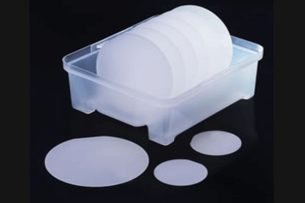
Our sapphire substrates come in both clear and frosted versions.
- All orientations are available, custom orientation is welcome
- Wafer size from 2 to 6 inches are available for all types
- Thin wafer down to 250um for 2 inch, 300um for 4 inch and 300um for 6 inch
Sapphire is a material of a unique combination of physical, chemical and optical properties, which make it resistant to high temperature, thermal shock, water and sand erosion, and scratching. It is a superior window material for many IR applications from 3µm to 5µm. C-plane sapphire substrates are widely used to grow III-V and II-VI compounds such as GaN for blue LED and laser diodes, while R-plane sapphire substrates are used for the hetero-epitaxial deposition of silicon for microelectronic IC applications.
Applications of Sapphire substrates:
- Growth substrate for III-V and II-VI compounds
- Electronics and optoelectronics
- IR applications
- Silicon On Sapphire Integrated Circuit(SOS)
- Radio Frequency Integrated Circuit(RFIC)
Description of our Sapphire substrates
Sapphire is a crystalline form of aluminum oxide (Al2O3) and is extremely unreactive and chemically-resistant to acids and alkalis, including hydrofluoric acid. Furthermore, sapphire is exceptionally hard with a Moh’s hardness of 9, (compared to diamond = 10 and glass ~5.5). These substrates are therefor very scratch-resistant. Last but not least it can withstand high temperatures, has high thermal conductivity, does not degrade under UV light, and features a high dielectric strength.These characteristics, and many more, make sapphire a preferred premium material for many applications in photonics, solid-state lighting, scientific research, lenses and covers, design lighting, optical sensors, and many, many more where the environmental conditions are demanding.
Our sapphire substrates come in both clear and frosted versions. If you are in need of different dimensions or thicknesses, or if you have a high volume demand. Please contact us for a quote.
Specification:
| Orientation | R-plane, C-plane, A-plane, M-plane or a specified orientation | ||
| Orientation Tolerance | ± 0.3° | ||
| Diameter | 2 inches, 3 inches, 4 inches, 6 inches, 8 inches or others | ||
| Diameter Tolerance |
0.1mm for 2 inches, 0.2mm for 3 inches, 0.3mm for 4 inches, 0.5mm for 6 inches |
||
| Thickness | 0.25mm, 0.33mm, 0.43mm, 0.65mm, 1mm or others; | ||
| Thickness Tolerance | 25μm | ||
| Primary Flat Length |
16.0±1.0mm for 2 inches, 22.0±1.0mm for 3 inches, 30.0±1.5mm for 4 inches, 47.5/50.0±2.0mm for 6 inches |
||
| Primary Flat Orientation |
A-plane (1 1-2 0 ) ± 0.2°; C-plane (0 0-0 1 ) ± 0.2°, Projected C-Axis 45 +/- 2° |
||
| TTV |
≤10µm for 2 inches, ≤15µm for 3 inches, ≤20µm for 4 inches, ≤25µm for 6 inches |
||
| BOW |
≤10µm for 2 inches, ≤15µm for 3 inches, ≤20µm for 4 inches, ≤25µm for 6 inches |
||
| Front Surface | Epi-Polished (Ra< 0.3nm for C-plane, 0.5nm for other orientations) | ||
| Back Surface | Fine ground (Ra=0.6μm~1.4μm) or Epi-polished | ||
| Packaging | Packaged in a class 100 clean room environment | ||
Single crystal Sapphire is a material of a unique combination of physical, chemical and optical properties.
Sapphire substrates are ideal for use instead of glass substrates(Sapphire substrates is exceptionally hard with a Mohs hardness of 9, second only to diamond (which has a hardness of 10). For comparison, glass substrates has a hardness of ~5.5. This makes it extremely scratch-resistant.) when optical transmission is required in the ultraviolet (above 200 nm) or infrared (below 5 μm) range. Low-temperature optical measurements will also benefit from the higher thermal conductivity of sapphire substrates, and they may also be used in high temperature environments up to 2300 K.
Sapphire substrate has many exceptional properties of high hardness, high strength, scratch resistance, low dielectric loss good electrical insulation, high temperature resistance, chemical durability and excellent transmission bandwidths. Sapphire substrate plays an important role in opto-electronics industry and widely used in precision mechanical parts and vacuum equipment.
Sapphire substrate can be offered in round shape, square shape and custom shape. Our achievable diameter is up to 400mm, ultra-thin substrate is as thin as 80 microns in thickness.
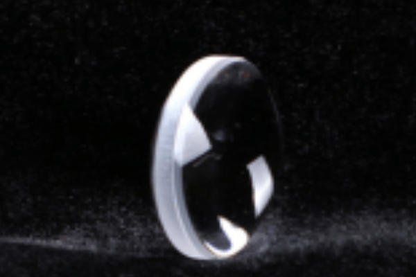
Sapphire BCX Lens

Sapphire Rectangle Windows

Sapphire Circular Windows
What are Sapphire Substrates?
Manufacturers produce sapphire substrates from single-crystal aluminum oxide (Al2O3), often known as sapphire, because of their transparent and durable qualities. These substrates form the foundation for various semiconductor devices, optoelectronics and micro-electromechanical systems (MEMS). Renowned for their superior thermal, electrical and optical properties, sapphire substrates provide a high-quality surface for epitaxial growth, which is vital in producing high-performance devices.
What Applications Are Sapphire Substrates Used For?
Sapphire substrates find extensive applications in numerous high-tech industries. They are fundamental in producing semiconductor devices, where their thermal stability and electrical insulation properties offer substantial advantages. In optoelectronics, sapphire’s transparency and high refractive index make it an excellent choice for GaN-based LEDs, where the Patterned Sapphire Substrates (PSS) technique has boosted their efficacy. Furthermore, Micro-Electro-Mechanical Systems (MEMS) technology also uses sapphire substrates for devices like accelerometers, gyroscopes and micro-mirrors due to its superior mechanical strength and chemical resistance.
What are the advantages of sapphire substrate?
Sapphire has exceptional electrical insulation, transparency, good thermal conductivity, and high rigidity properties. Hence it is an ideal material for substrates and is used in LED and microelectronic circuits, ultra-high-speed integrated circuits.
What is patterned sapphire substrate?
Patterned Sapphire Substrates (PSS) is micro-patterned sapphire substrate used to for GaN based light emitting diodes(LEDS). The PSS reduces the dislocation density in the GaN layer, enhances the light extraction efficiency and increase LEDs' brightness.
What is the absorption of sapphire substrate?
At a wavelength < 300 nm, there is a high peak absorptance for the sapphire. While the absorptance is very low from 300 to 1200 nm, particularly in IR light. This means deep UV light is superior for the sapphire absorption.